Stage-1: the 10W PA
This is the technical description of the 10 watts power amplifier for es'hail-2, we call it the Stage-1 amplifier.
The prototype works quite well, so the next step is to make the final layout by adding some additional circuits, mainly the PTT circuit which allows to switch OFF the quiescent current during RX periods. This saves power and reduces the temperature of the amplifier.
(The data for the prototype are available HERE for people who own the prototype board), everybody else better use this final circuit and layout).
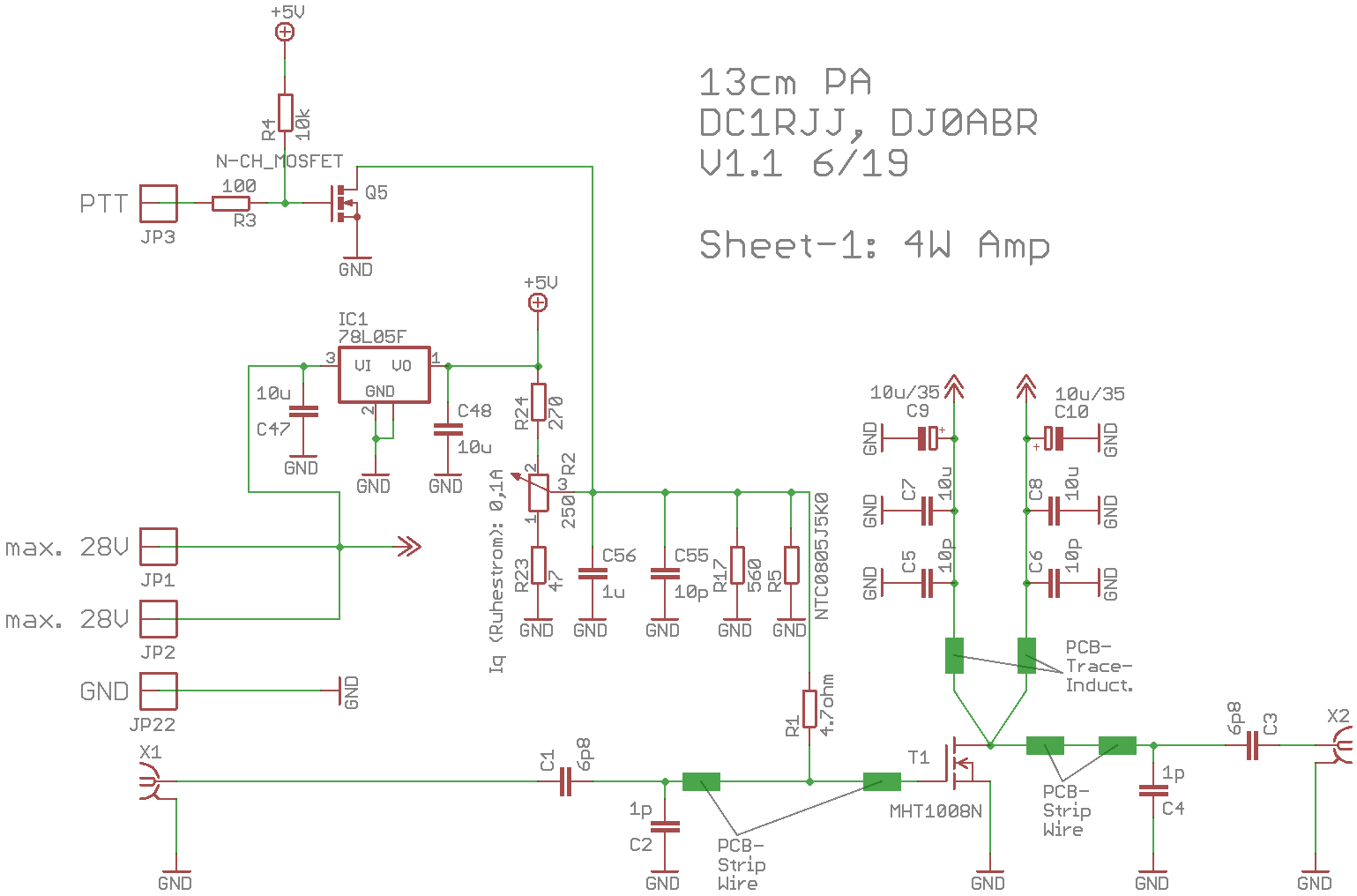
Schematics (click for a larger view):
Circuit description:
The input has a DC block capacitor C1 followed by the input matching network. This match is done by the copper plane at the transistor gate pin together with C2. Four additional stripline capacitor planes are located directly at the input match stipline. One of them is connected by default. In some cases it may be required to connect a second one. This will not improve the output of the amplifier, but it can improve the input match and the gain.
The gate voltage is ganerated by a 78L05 voltage regulator followed by a resistor network with an NTC which is used to stabilize the quiescent current. Many voltage regulators may be used, but take care that the regulator can handle the maximum input voltage of the amplifier (most LDOs are limited to abt. 20V !).
In RX mode we do not need any quiescent current. If the PTT is unconnected or "logic high", then Q5 short cuts the gate voltage to GND and the Mosfet transistor is switched off. In TX mode PTT will be low (GND) and the transistor gets the gate voltage and is operational.
The ouput of the transistor's drain is connected to a two-stage micro stip mathing network together with C4 and followed by the DC decoupling capacitor C3.
The supply voltage is fed to the transistor via two similar lines. This is a recommendation of the reference layout for low impedance power supply. Please connect both 24V pads in parallel to your power supply.
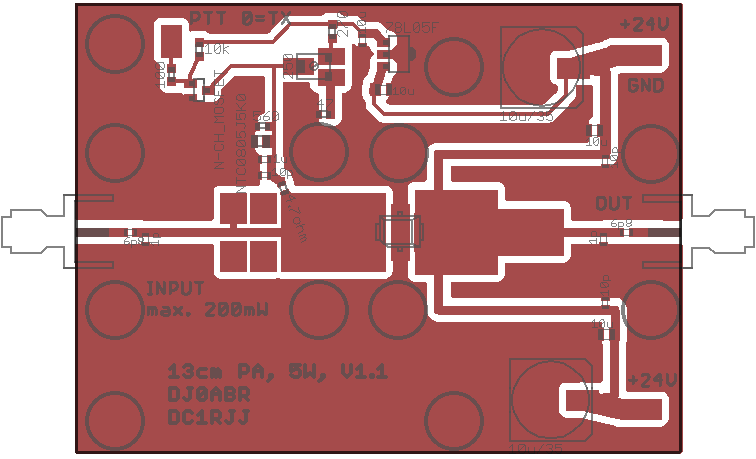
Layout:
Building hints:
solder the SMA connectors directly, and as close as possible, to the board. It is NOT sufficiant to use a metal housing as a ground connection !
The board must be screwed directly to a cooler. Before soldering the board use fine sand paper to make the bottom of the board flat, remove all rough edges, be carefully, don't remove to much material from the ground plane, just the rough parts.
Screw the board to cooler a using 12 screws, use ALL of them, this is very important !
It may be required to remove some material from the cooler (using a file or drill) at the location of the SMA connectors, since they are soldered on the bottom side of the PCB. The PCB must be mounted flat and in good contact to the cooloer.
Optinally: A good practise is to remove the black anodic coating from the cooler using sand paper.
Use some (not too much) thermal compound.
Mounting the LDMOS transistor:
the MOSFET dissipates the heat through the vias of the PCB to the cooler.
Therefore the bottom of the transistor MUST be soldered to the board. This is not possible with a soldering iron. Instead apply some solder paste to the board (abt. 0.1mm to 0.2mm), place the MOSFET into this paste and then put it into an oven until the solder paste melts. In case of questions about this process watch the Youtube videos about hobby SMD soldering using the kitchen stove, a toaster or other alternatives.
Commissioning:
First of all: I am NOT responsible for any damage or malfunction. If you build this amplifier you should know what you are doing and you are responsible by yourself. All documents are release under the GNU public license v3 (see HERE).
The PTT input should be connected to the PTT output of your transceiver.
if you own some test equipment it's now time to feed in a 2,4 GHz signal and check the output.